Researchers at George Washington University recently invented an optical switching technology for future photonics network-on-chip (NOC). This invention enables compact, cost-effective two orders of magnitude increases in bandwidth and dramatically more energy-efficient communication between CPU’s compared to traditional electrical interconnects. Photonics-based communication is the backbone of the internet. The trend over the last 10 years is to steadily expand the applications domain of photonics into shorter distances e.g. from long haul communications (~100% photonics) to residential applications (< 20%), and finally to inter-machine (i.e. computer) communication (<1%, currently, but growing). The current frontier use is optical/photonic communications inside data centers and servers. For example, Intel Corporation had an announcement with Facebook last year to revolutionize data centers by linking multiple servers (within a rack) with optical/photonic communications.
The motivation is three-fold:
- Photonics offers superior (~ 100x) data bandwidth over electrical connections via Wave Division Multiplexing (WDM) (simultaneous usage of multi-color light)
- Photonics uses 10-100x less power per bit of information for distances beyond ~ 0.2 mm
- Device footprint is now compact enough to be practical for inter-machine and within machine applications.
Fig. 1
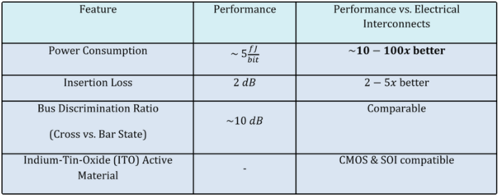
Fig. 2
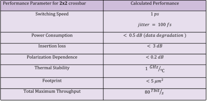
Fig. 3
Technical Features:
The 2x2 electro-optic switch replaces electrical interconnects, and operates with ultra-low power consumption. Key figures of merit are seen in Figure 2 (located in the image gallery on right).
Technologically photonics is the next evolutionary step for computing architectures. Researchers believe that photonic communication will eventually migrate to laptops and even smart phones. Economically, it offers high a competitive edge via both dramatically higher speeds at dramatically lower power.The device is CMOS compatible, and can be seamlessly integrated into a SOI (silicon on insulator) technology platform. The active material is Indium-Tin-Oxide (ITO), and a material processing database is available. The internal device physics relies on a hybrid plasmon mode, whose effective refractive index is altered electrically.
The performance parameters can be estimated for a 2x2 crossbar switch based on the disclosed device are seen in Figure 3 (located in the image gallery on right).