As computer chip feature size continue to decrease, power consumed due to on-chip communications will dramatically grow. This calls for new techniques which can provide higher bandwidth and data rates than over traditional electrical interconnects.
Photonic interconnects can provide higher bandwidth and data rates. However optoelectronic devices generally require more power and a large footprint. Conversely, plasmonic interconnects can provide energy efficiency and small footprint, but have lower bandwidth and data rates. To overcome these problems the George Washington University (GW) inventors designed hybrid photonic and plasmonic interconnects that retain the best features of both individual solutions. The GW inventors then modeled hybrid performance against pure photonic and pure plasmonic interconnects. Hybrid interconnects are better in terms of point-to-point latency and energy consumption as shown by the graphs below.
Point-to-point latency: Time required for the propagation of a single bit from one light source across the link to detection by the photoreceiver.
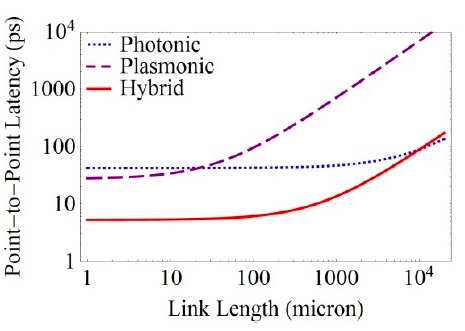
FIG. 1 - Point-to-Point Latency
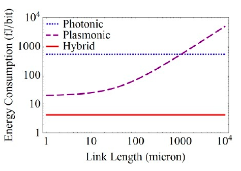
FIG. 2 - Energy Consumption
Applications:
- Communication links in optical circuits including processors/co-processors
- Large organizations with many computer systems
- Servers with many service requests
Advantages:
- Speed: outperforms traditional electrical interconnects
- Energy-efficient