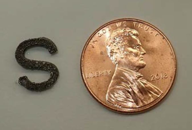
Researchers at the George Washington University have invented a novel additive manufacturing technique for fabrication of semiconductor and thermoelectric structures of various shapes and sizes, as required for specific electronic and thermoelectric applications, via selective laser melting (also known as laser powder bed fusion and direct metal laser sintering). The additive manufacturing technique has been used to build thermoelectric materials in a layer by-layer fashion in various shapes and sizes by using powders as starting materials. The thermoelectric materials have important technology and commercial application as miniature coolers for electronic components of various computing and mobile systems, such as data centers, server farms, personal computers, smart phones, etc.
Thermoelectric semiconductor devices have unique advantages for thermal to electrical energy conversions or electrical to thermal energy conversions. As heat engines, thermoelectric generators can directly generate electricity from waste heat via the Seebeck effect. Thermoelectric coolers provide solid state cooling through the Peltier effect. Both thermoelectric generators and coolers have no mechanically moving parts, so they are more compact than standard power generation and refrigeration systems. Despite these advantages, thermoelectric devices have failed to become widespread in energy efficiency and thermal management applications in part because current manufacturing processes utilize a complex set of traditional manufacturing techniques, which limits device design and adaptability. Additionally, current production methods generally result in materials exhibiting low energy conversion efficiencies.
The additive manufacturing techniques based on selective laser sintering methods developed by the GW researchers are capable to overcome the difficulties associated with manufacturing devices based on thermoelectric materials such as thermoelectric coolers.
We believe that this technology will soon provide a reliable solution to the thermal management problem in various telecommunications and computing systems such as personal devices, data centers, server farms, and high performance computing.
Applications:
1. Thermoelectric materials fabrication
2. Semiconductor fabrication
3. Cooling of computer hardware
Advantages:
1. Fabrication of thermoelectric structures having the shapes and sizes required for specific electronic and thermoelectric applications (eliminates several difficult subsequent material processing steps